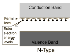
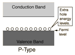
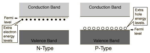
Bands for Doped Semiconductors

The application of band theory to n-type and p-type semiconductors shows that extra levels have been added by the impurities. In n-type material there are electron energy levels near the top of the band gap so that they can be easily excited into the conduction band. In p-type material, extra holes in the band gap allow excitation of valence band electrons, leaving mobile holes in the valence band.

Click on either case for further details.
Index

Semiconductor concepts

Semiconductors for electronics
 
HyperPhysics***** Condensed Matter R Nave
Go Back


N-Type Band Structure

The addition of donor impurities contributes electron energy levels high in the semiconductor band gap so that electrons can be easily excited into the conduction band. This shifts the effective Fermi level to a point about halfway between the donor levels and the conduction band.

Electrons can be elevated to the conduction band with the energy provided by an applied voltage and move through the material. The electrons are said to be the "majority carriers" for current flow in an n-type semiconductor.

Index

Semiconductor concepts

Semiconductors for electronics
 
HyperPhysics***** Condensed Matter R Nave
Go Back


P-Type Band Structure

The addition of acceptor impurities contributes hole levels low in the semiconductor band gap so that electrons can be easily excited from the valence band into these levels, leaving mobile holes in the valence band. This shifts the effective Fermi level to a point about halfway between the acceptor levels and the valence band.

Electrons can be elevated from the valence band to the holes in the band gap with the energy provided by an applied voltage. Since electrons can be exchanged between the holes, the holes are said to be mobile. The holes are said to be the "majority carriers" for current flow in a p-type semiconductor.

Index

Semiconductor concepts

Semiconductors for electronics
 
HyperPhysics***** Condensed Matter R Nave
Go Back