Junction Field Effect Transistor
 |
The common transistor is called a junction transistor, and it was the key device which led to the solid state electronics revolution. In application, the junction transistor has the disadvantage of a low input impedance because the base of the transistor is the signal input and the base-emitter diode is forward biased. Another device achieved transistor action with the input diode junction reversed biased, and this device is called a "field effect transistor" or a "junction field effect transistor", JFET. With the reverse biased input junction, it has a very high input impedance. Having a high input impedance minimizes the interference with or "loading" of the signal source when a measurement is made. |
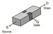 |
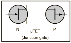
For an n-channel FET, the device is constructed from a bar of n-type material, with the shaded areas composed of a p-type material as a Gate. Between the Source and the Drain, the n-type material acts as a resistor. The current flow consists of the majority carriers (electrons for n-type material). |
Since the Gate junction is reverse biased and because there is no minority carrier contribution to the flow through the device, the input impedance is extremely high.
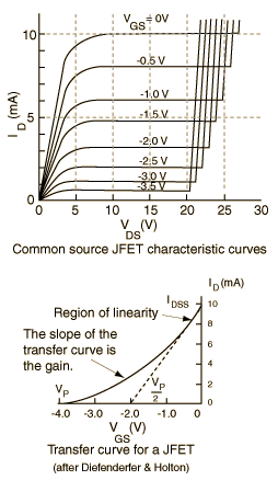
The control element for the JFET comes from depletion of charge carriers from the n-channel. When the Gate is made more negative, it depletes the majority carriers from a larger depletion zone around the gate. This reduces the current flow for a given value of Source-to-Drain voltage. Modulating the Gate voltage modulates the current flow through the device.
Electronics concepts
Transistor varieties
Reference
Diefenderfer & Holton
Sec 8-7
| HyperPhysics*****Electricity and magnetism | R Nave |
